How to choose a PCB design and manufacturing partner.
Choose a partner who understands the product, the work it needs and the evidence required for the next build. Ask how circuit and layout decisions, bring-up, manufacturing information and later changes would be handled.
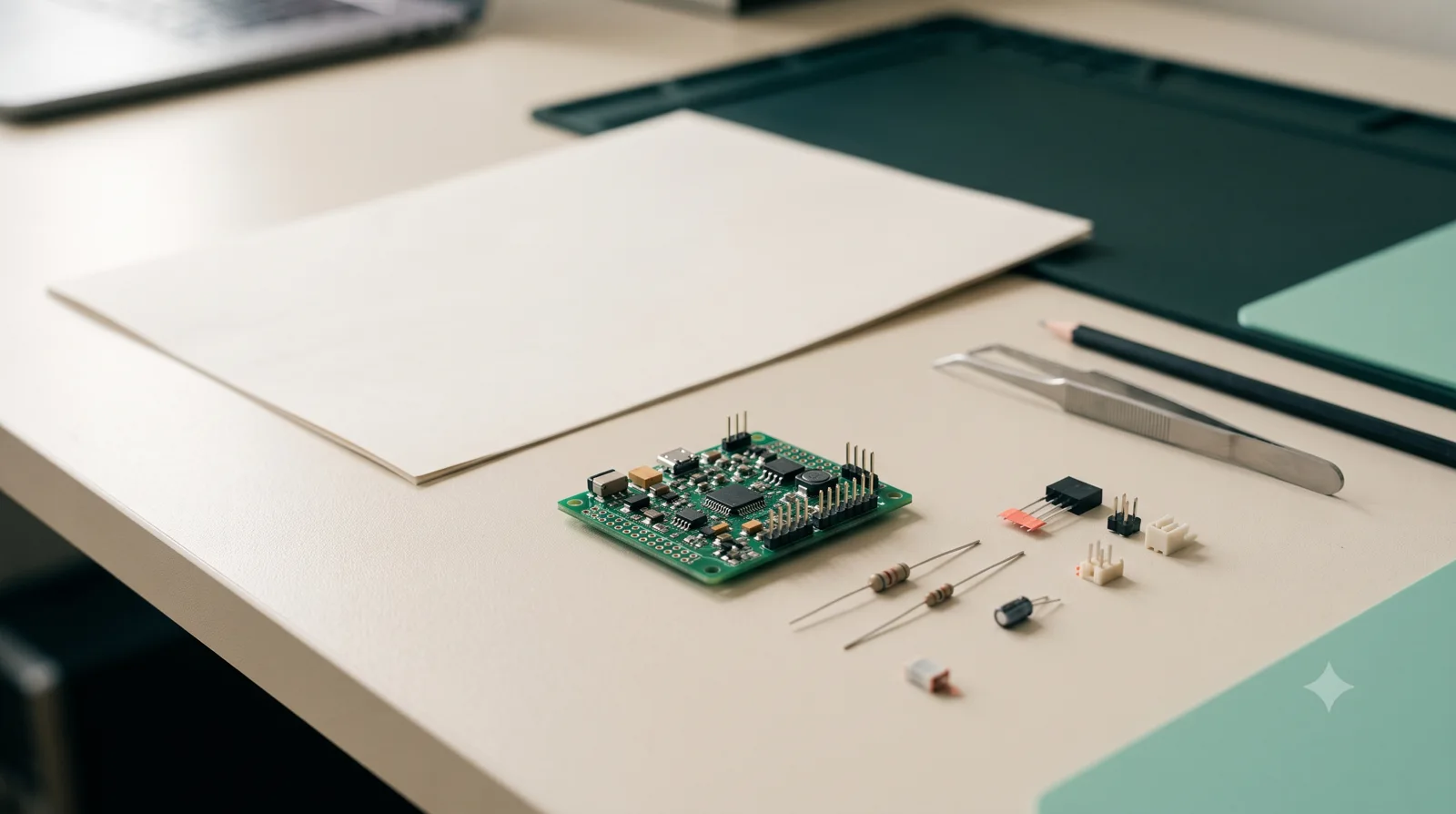
Clarify circuit and layout responsibility
Understand what is included in the design scope and what information the team expects. The product interfaces, power, physical constraints and manufacturing needs should inform the schematic and PCB discussion.
- Required functions and interfaces
- Schematic and PCB review responsibility
- Component and physical constraints
- Design-for-build and test considerations
Understand the bring-up and test approach
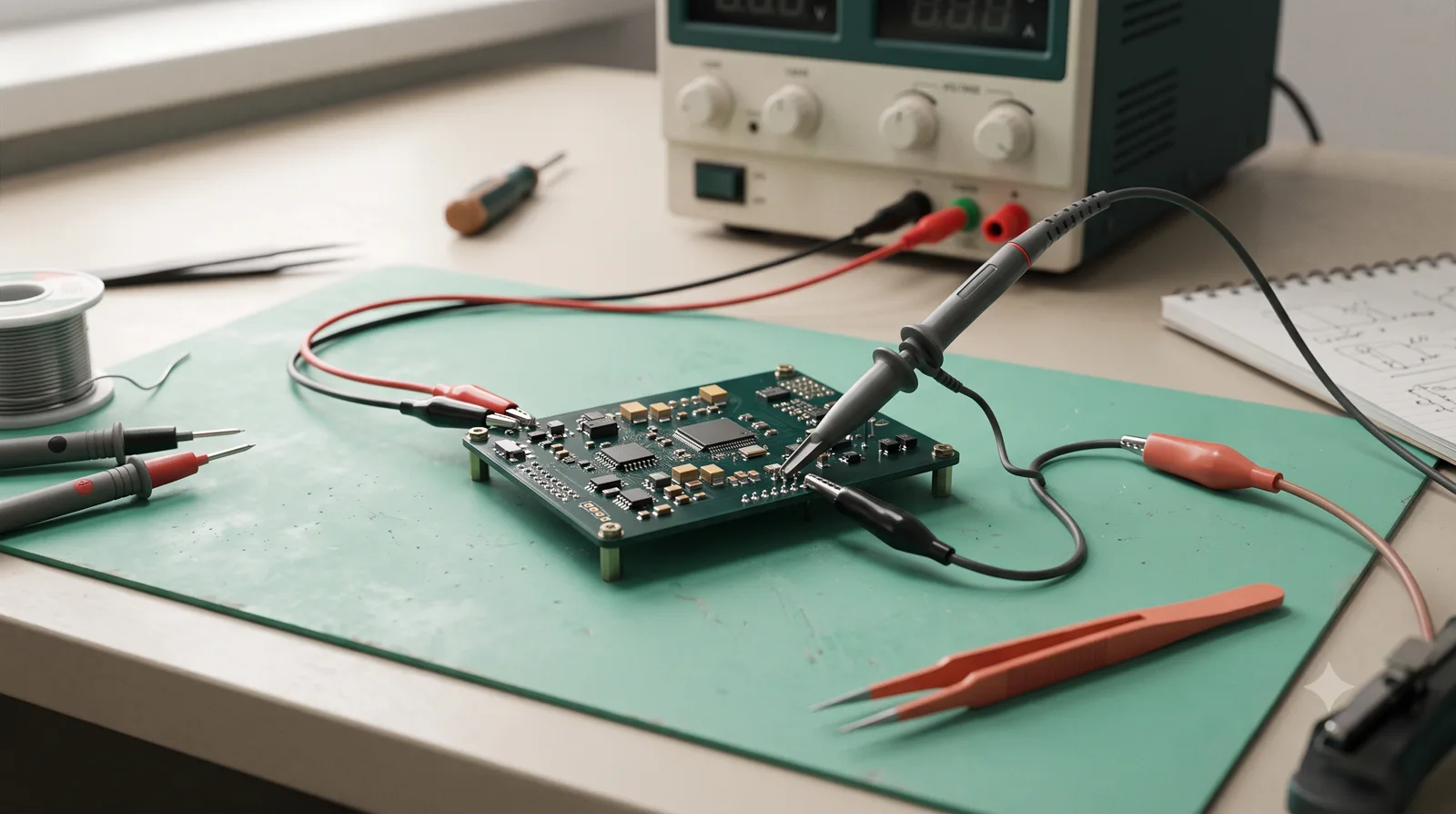
Ask how the first board would be assessed and how observations would be documented. A useful plan identifies relevant functions, configuration, test access and the issues that need to be resolved before the next revision or build.
- Agreed functional checks
- Configuration and test records
- How faults and limitations are reviewed
- What guides the next revision
Check manufacturing information and support
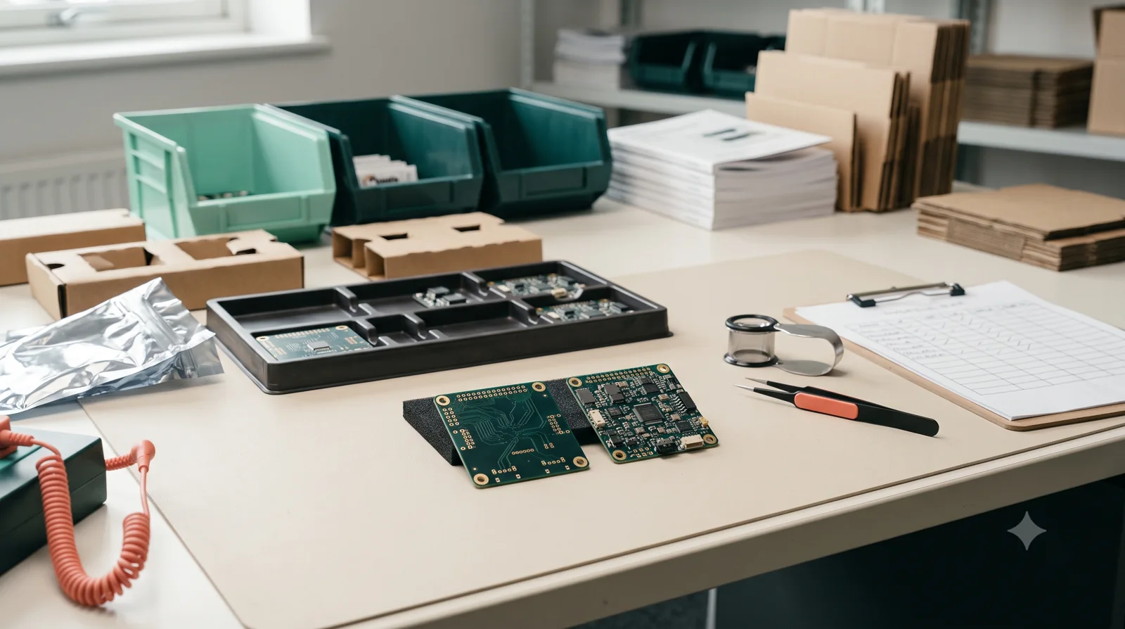
Clarify the files, component/BOM information, assembly/test notes and responsibilities included in the handoff. Keep engineering scope and PCB ordering distinct so the next action and the relevant release information are clear.
- Agreed design and manufacturing files
- BOM and component decisions
- Assembly and test guidance
- Release, support and future-change boundaries
Make the comparison concrete.
Use the same product requirement and build scope on both sides of the comparison. Ask for the information that helps your team make and support the decision.
| Compare | Ask or review | What the answer should clarify |
|---|---|---|
| Design responsibility | How will circuit, layout and interfaces be reviewed? | Relevant requirement and design-review scope. |
| Bring-up and test | What is checked on the first board? | Configuration, checks, findings and limitations. |
| Manufacturing information | What files and build guidance are included? | Agreed versions, BOM, assembly and test information. |
| Future changes | How will an issue or revision be handled? | Clear support and change responsibilities. |
Questions about the next step
What distinguishes design work from fabrication?
Design defines the electronics and board information. Fabrication produces the board from the agreed manufacturing package; assembly and configuration add further scope. Confirm which responsibilities the partner is taking.
What should a PCB partner handover include?
Agree the relevant editable design files, fabrication data, BOM/component information, placement/assembly data, firmware/configuration and test records for the engagement.
Continue your project
Make the next milestone a useful one.
Tell us what exists today, what needs to change and the decision your team needs to make. We’ll connect the discussion with the relevant engineering scope.