
TekRabbits production desk · configuration help
Understand the choices behind your board.
Short answers in the order flow, deeper guides when you want the engineering context, and clear diagrams for discussing each manufacturing choice.
 PCB setup
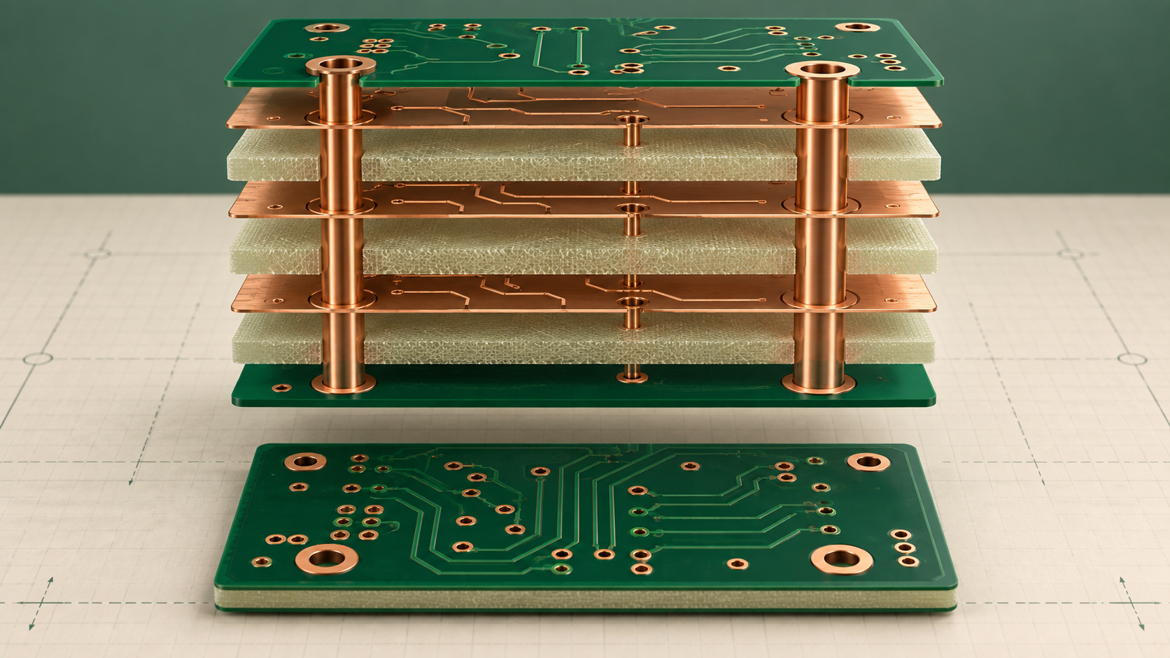
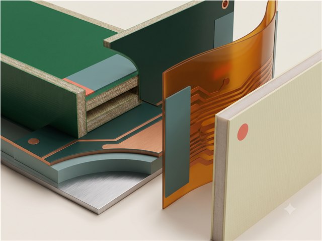
Base material
Choose the board family that supplies the mechanical and electrical foundation for the design.
Read the guide ↗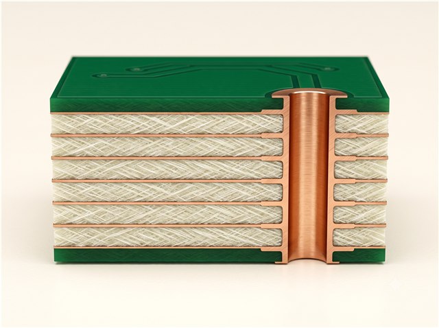 PCB setup
Layers
Set the number of copper layers your electrical and mechanical design needs.
Read the guide ↗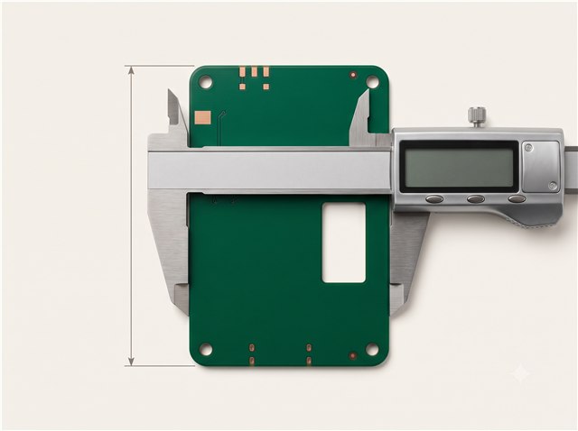 PCB setup
Board dimensions
Confirm the analysed outline size and keep the build aligned with the submitted design.
Read the guide ↗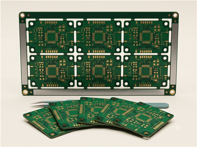 PCB setup
PCB quantity
Choose how many finished boards or panels the order should contain.
Read the guide ↗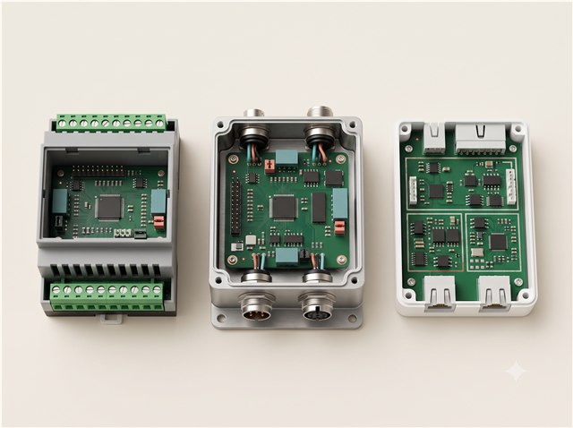 PCB setup
Product type
Describe the application context so the estimate is interpreted with the right quality expectations.
Read the guide ↗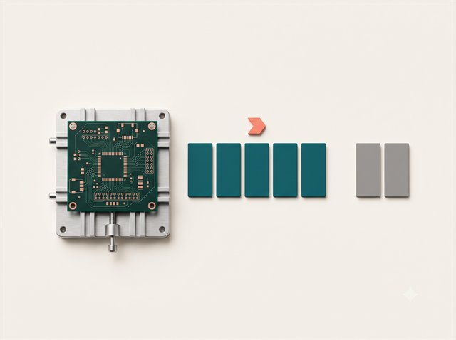 Order preference
PCB fabrication time
Choose the working-day option that fits the build schedule.
Read the guide ↗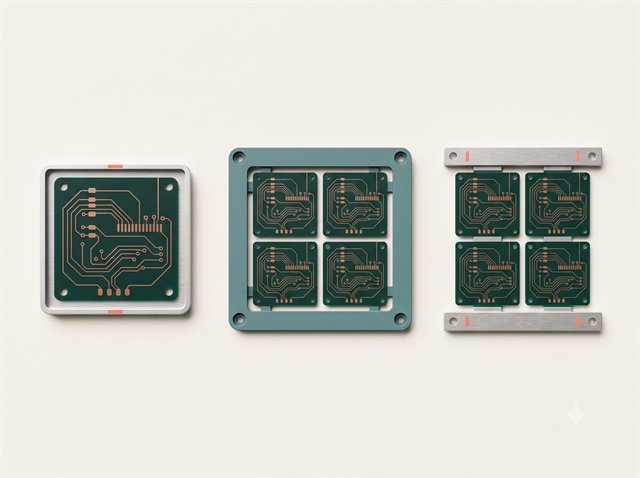 PCB basics
Delivery format
Tell us whether the delivered unit is a single board or a panelled format.
Read the guide ↗ PCB basics
PCB thickness
Choose a finished thickness that fits the enclosure and electrical stack-up.
Read the guide ↗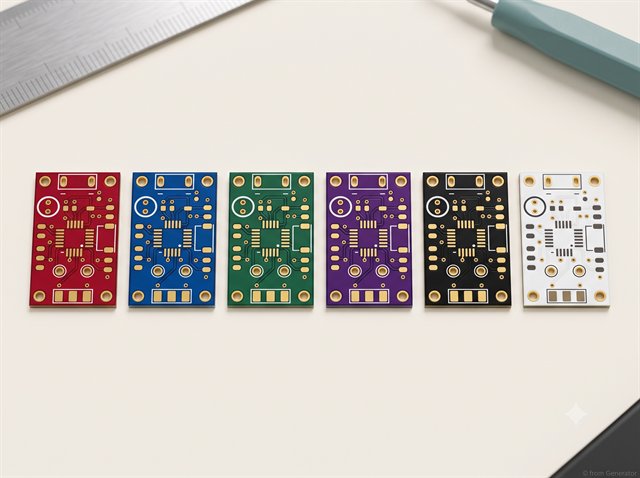 PCB basics
PCB colour
Choose the solder-mask colour that fits inspection and product identity.
Read the guide ↗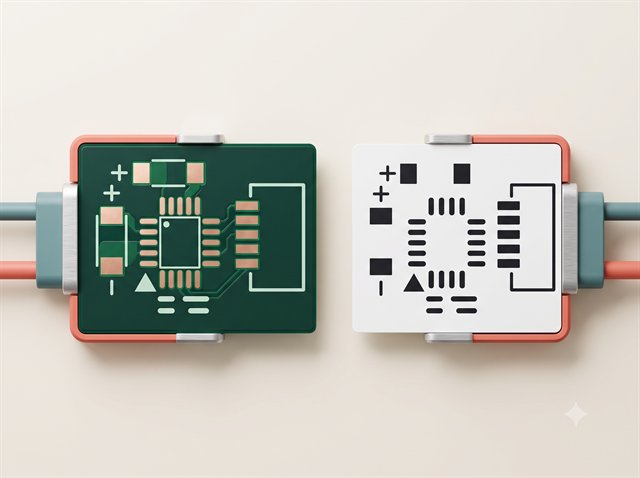 PCB basics
Silkscreen
Use the legend colour that gives clear markings against the selected solder mask.
Read the guide ↗ PCB basics
Material type
Choose the compatible laminate grade when the design needs a particular characteristic.
Read the guide ↗ PCB basics
Surface finish
Choose how exposed copper pads should be protected and prepared for soldering.
Read the guide ↗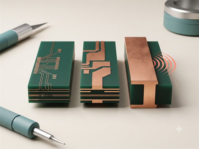 PCB basics
Outer copper weight
Set the copper thickness needed for current, heat and mechanical reliability.
Read the guide ↗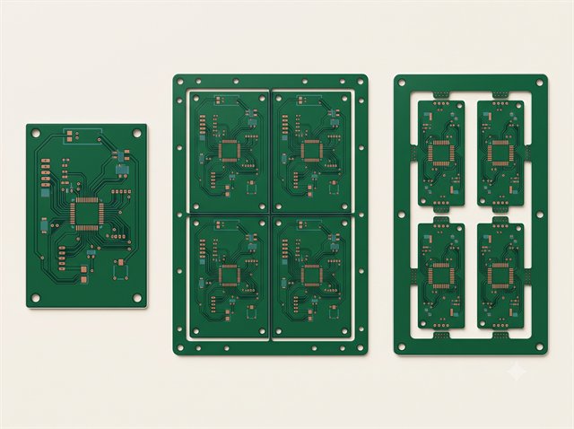 PCB advanced specifications
Panelisation
Choose whether the order is delivered as individual boards or a production panel.
Read the guide ↗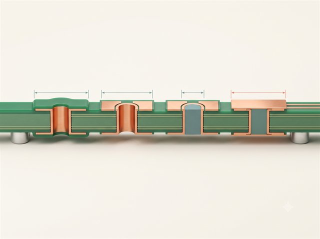 PCB advanced specifications
Via covering
Choose how via openings should be protected or filled.
Read the guide ↗ PCB advanced specifications
Via plating method
Specify a via-plating process only when the design needs it.
Read the guide ↗ PCB advanced specifications
Minimum via hole
Choose the smallest via geometry while respecting the analysed board.
Read the guide ↗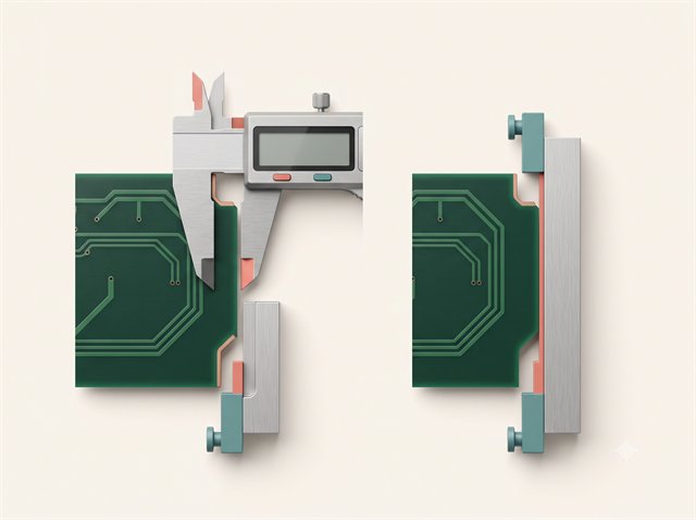 PCB advanced specifications
Board outline tolerance
Choose how closely the finished outline must follow the drawing.
Read the guide ↗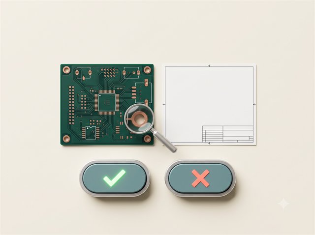 PCB advanced specifications
Confirm production file
Choose whether the production package receives an explicit confirmation step.
Read the guide ↗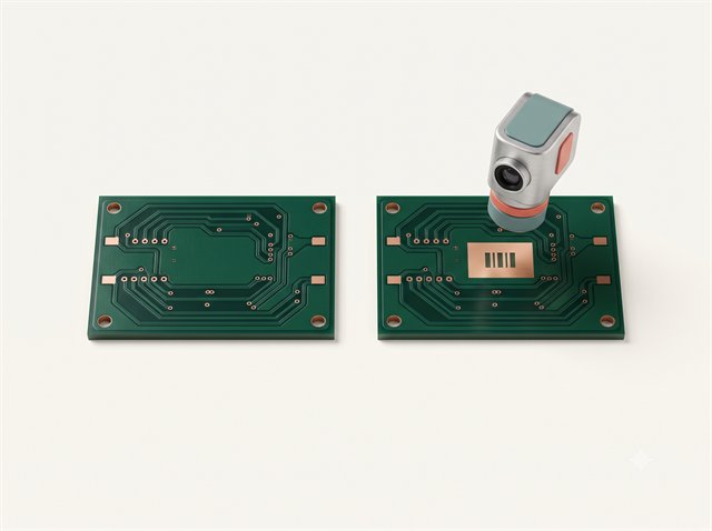 PCB advanced specifications
Mark on PCB
Decide whether the manufactured board needs a traceability mark.
Read the guide ↗ PCB advanced specifications
Electrical test
Select the electrical verification level appropriate for the build.
Read the guide ↗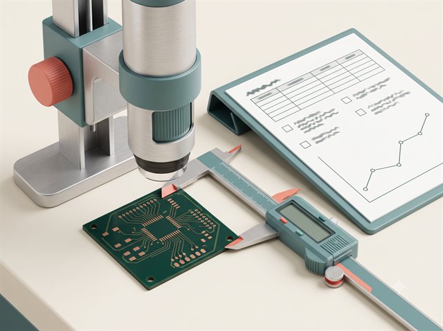 PCB advanced specifications
Inspection report
Request the inspection evidence that matches the acceptance plan.
Read the guide ↗ Order hand-off
Special instructions
Capture the few build requirements that structured options cannot express.
Read the guide ↗ PCB assembly
Assembly type
Choose the assembly path that matches the board, component data and production intent.
Read the guide ↗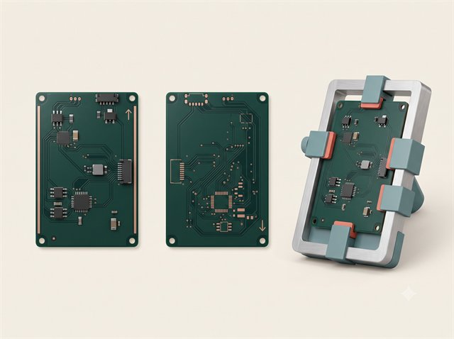 PCB assembly
Assembly side
Tell the assembly process which board faces carry components.
Read the guide ↗ PCB assembly
Assembly quantity
Choose how many boards should receive components.
Read the guide ↗ Traceability
Barcode / serial number settings
Configure a production-generated board identifier for service and traceability.
Read the guide ↗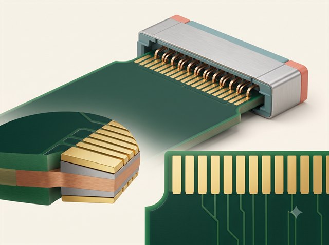 PCB advanced specifications
Gold fingers
Design durable plated edge contacts for the intended connector.
Read the guide ↗ PCB advanced specifications
Castellated holes
Prepare edge half-holes for solder-down modules.
Read the guide ↗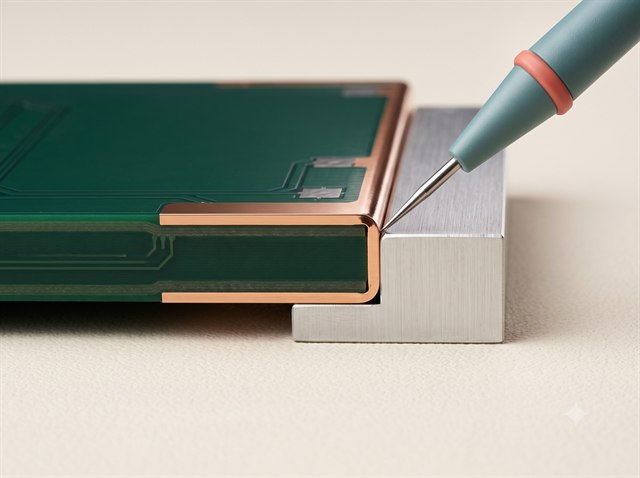 PCB advanced specifications
Edge plating
Define conductive board edges for shielding, grounding or contact.
Read the guide ↗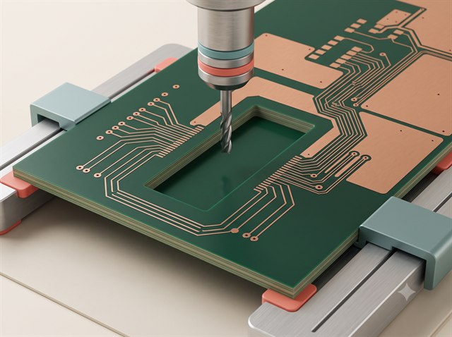 PCB advanced specifications
Blind slots
Specify controlled-depth routed recesses without ambiguity.
Read the guide ↗ Advanced options
UL marking
Understand when a recognised compliance mark may be used.
Read the guide ↗ Advanced options
Humidity indicator card
Add a visible moisture-exposure indicator to controlled packaging.
Read the guide ↗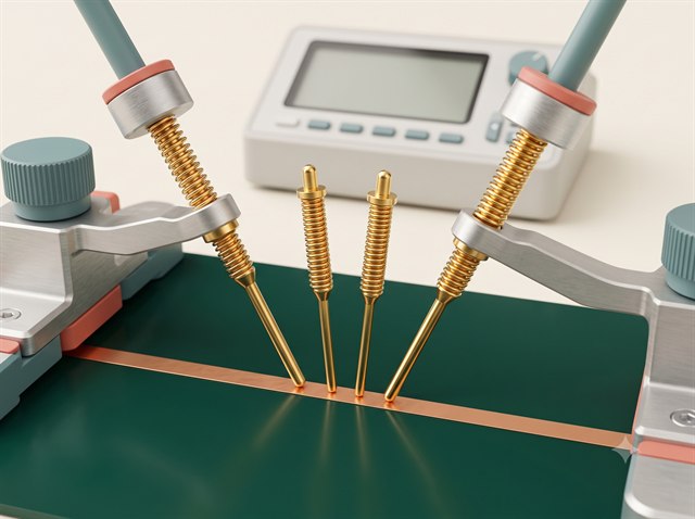 Advanced options
4-wire Kelvin test
Measure low resistance without lead and probe resistance dominating.
Read the guide ↗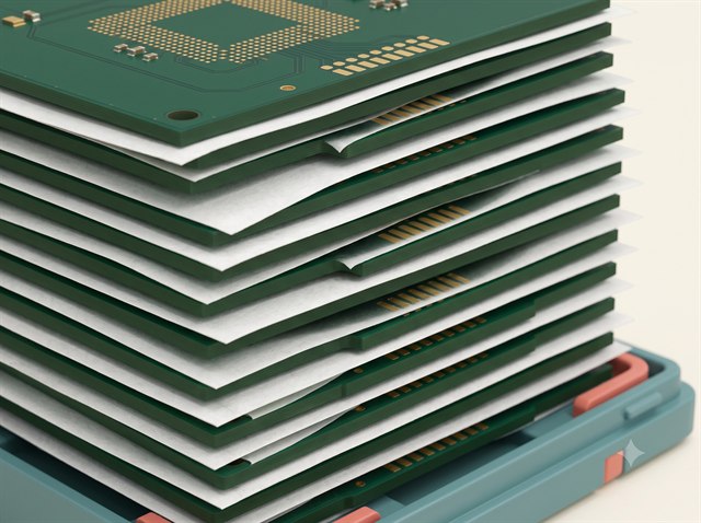 Advanced options
Paper between PCBs
Separate finished boards when cosmetic rubbing is a concern.
Read the guide ↗ Advanced options
Appearance quality
Set objective cosmetic expectations for visible board surfaces.
Read the guide ↗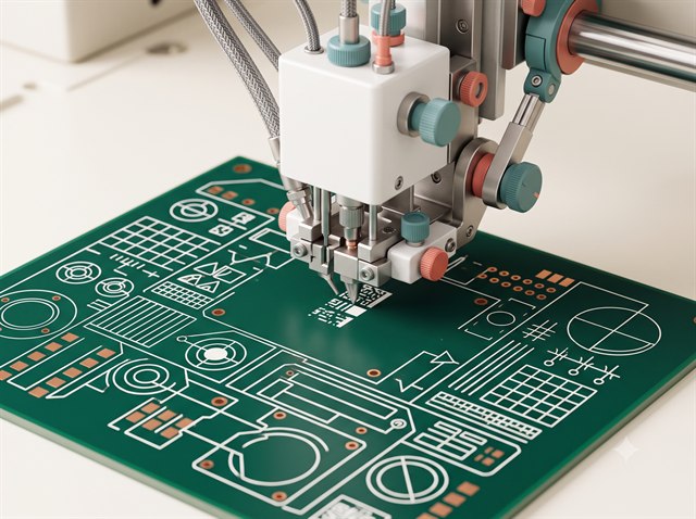 Advanced options
Silkscreen technology
Match the legend process to artwork size and readability.
Read the guide ↗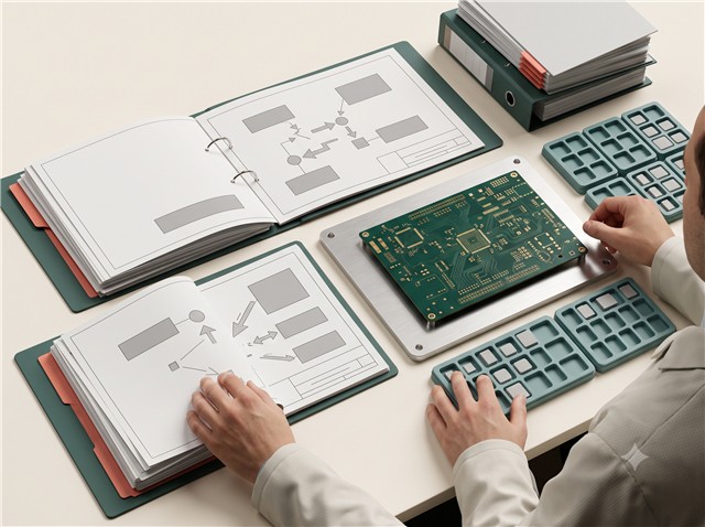 PCB assembly
Assembly instructions
Write concise, measurable requirements tied to released documents.
Read the guide ↗ PCB assembly
Tooling holes
Create repeatable datums for fixtures and assembly equipment.
Read the guide ↗ PCB assembly
Confirm parts placement
Review interpreted coordinates, rotations, polarity and side.
Read the guide ↗ PCB assembly
Stencil storage
Decide whether a revision-specific stencil should be retained.
Read the guide ↗ PCB assembly
Fixture storage
Retain controlled test or assembly tooling for repeat builds.
Read the guide ↗ PCB assembly
Parts selection
Assign responsibility for exact parts and approved substitutes.
Read the guide ↗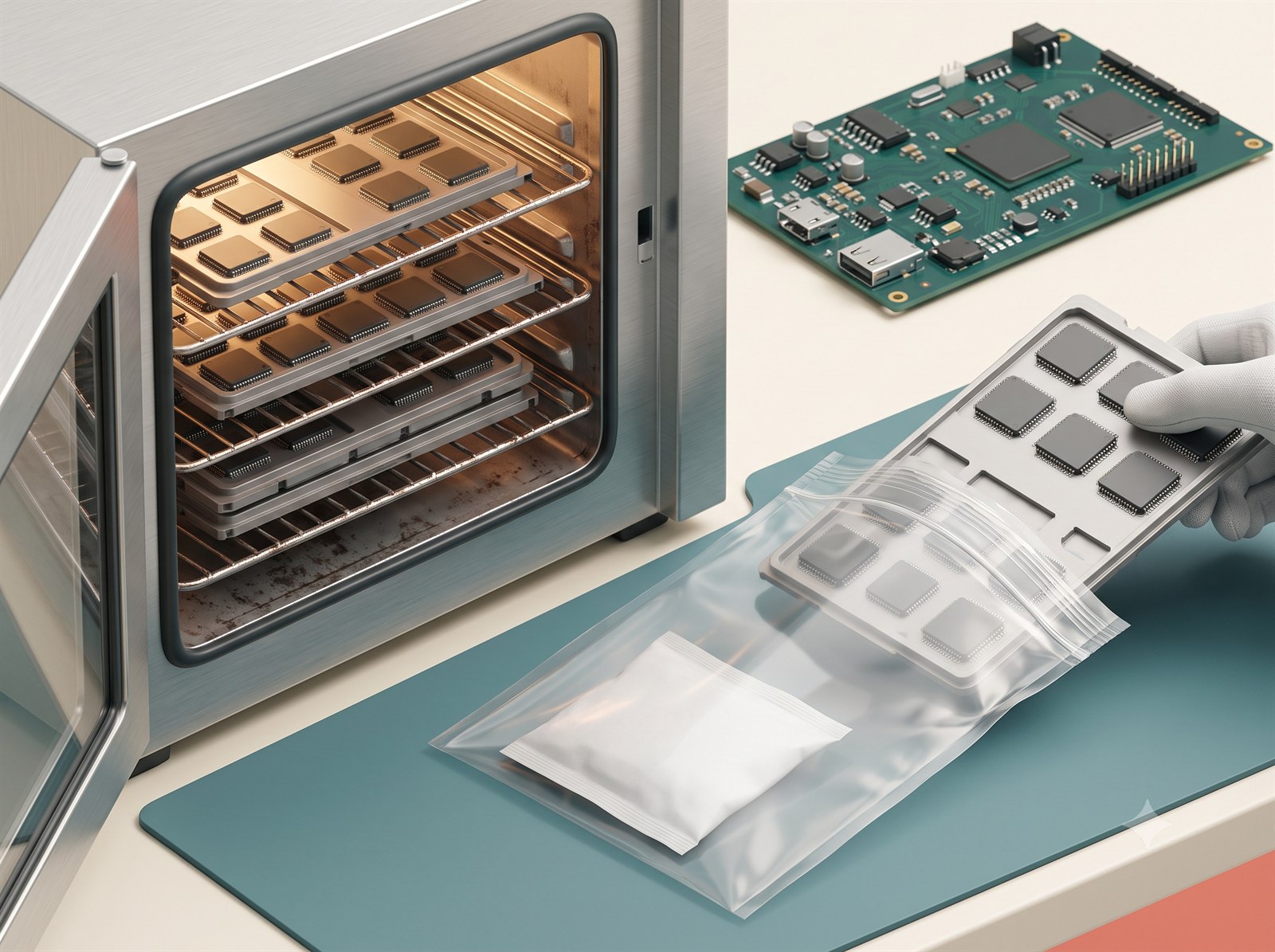 PCB assembly service
Bake components
Handle moisture-sensitive components using controlled requirements.
Read the guide ↗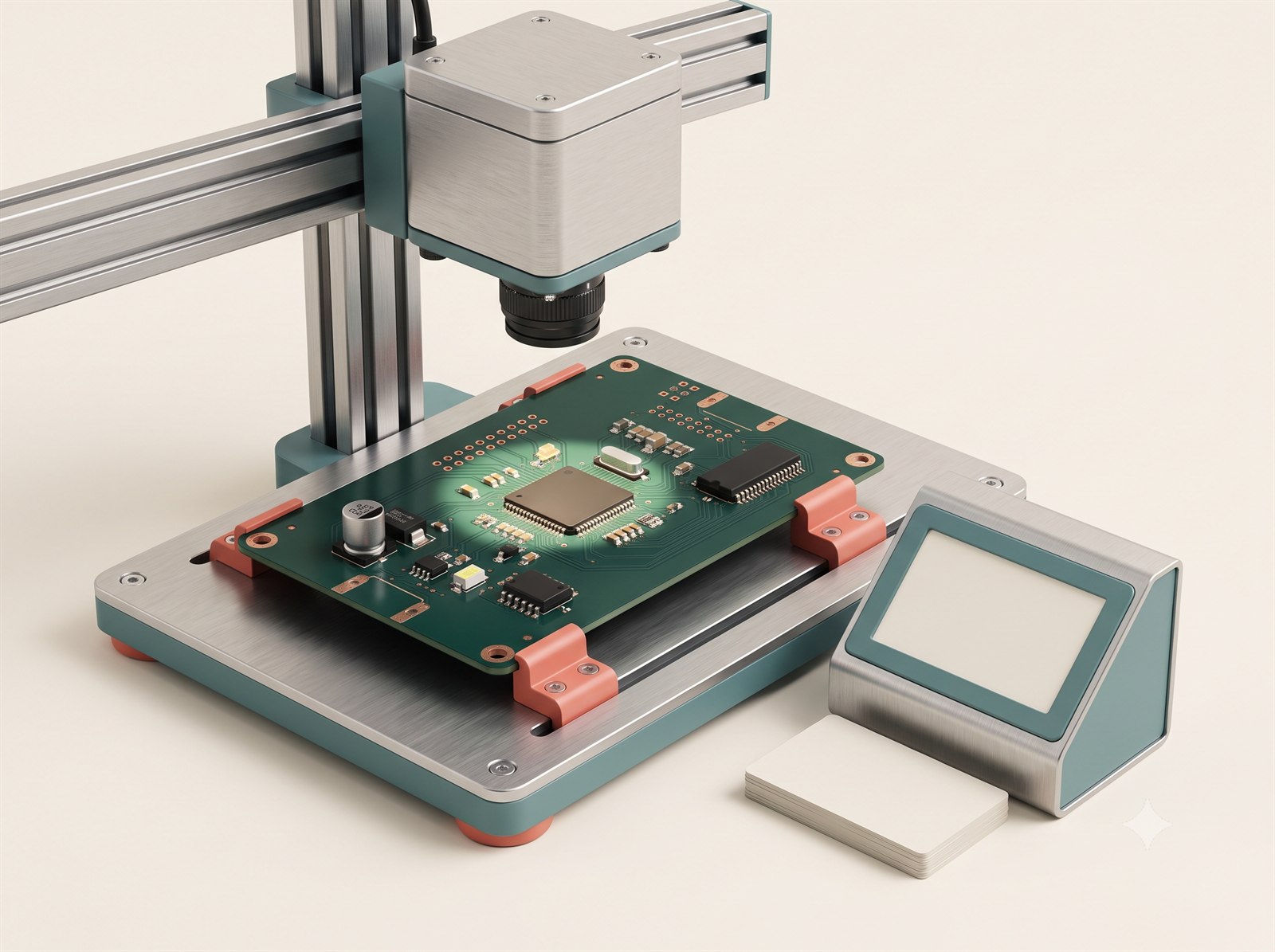 PCB assembly service
Photo confirmation
Use a visual checkpoint with a defined acceptance purpose.
Read the guide ↗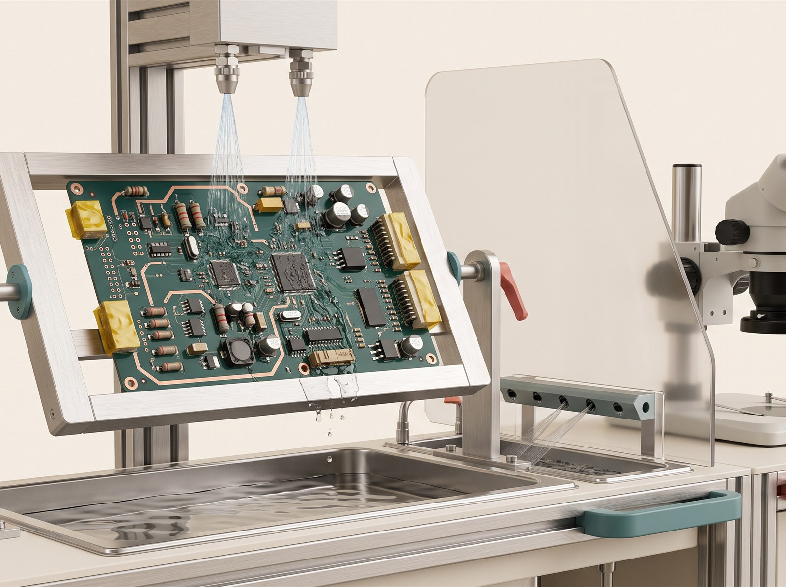 PCB assembly service
Board cleaning
Select a residue-removal method compatible with the assembly.
Read the guide ↗ PCB assembly service
Conformal coating
Define coating chemistry, sides, thickness and keep-outs.
Read the guide ↗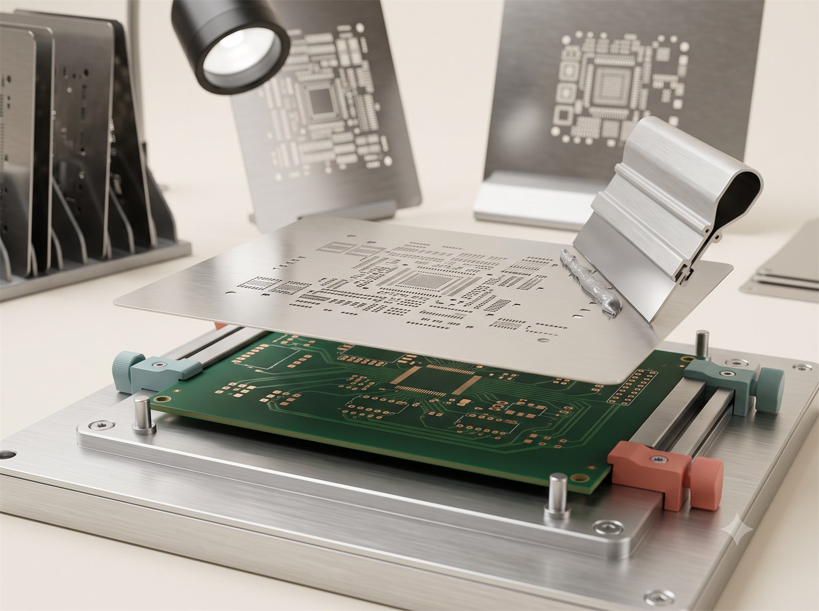 PCB assembly service
Special stencil
Control solder-paste deposits for a demanding component mix.
Read the guide ↗ PCB assembly service
Packaging
Protect finished assemblies from ESD, moisture and transit damage.
Read the guide ↗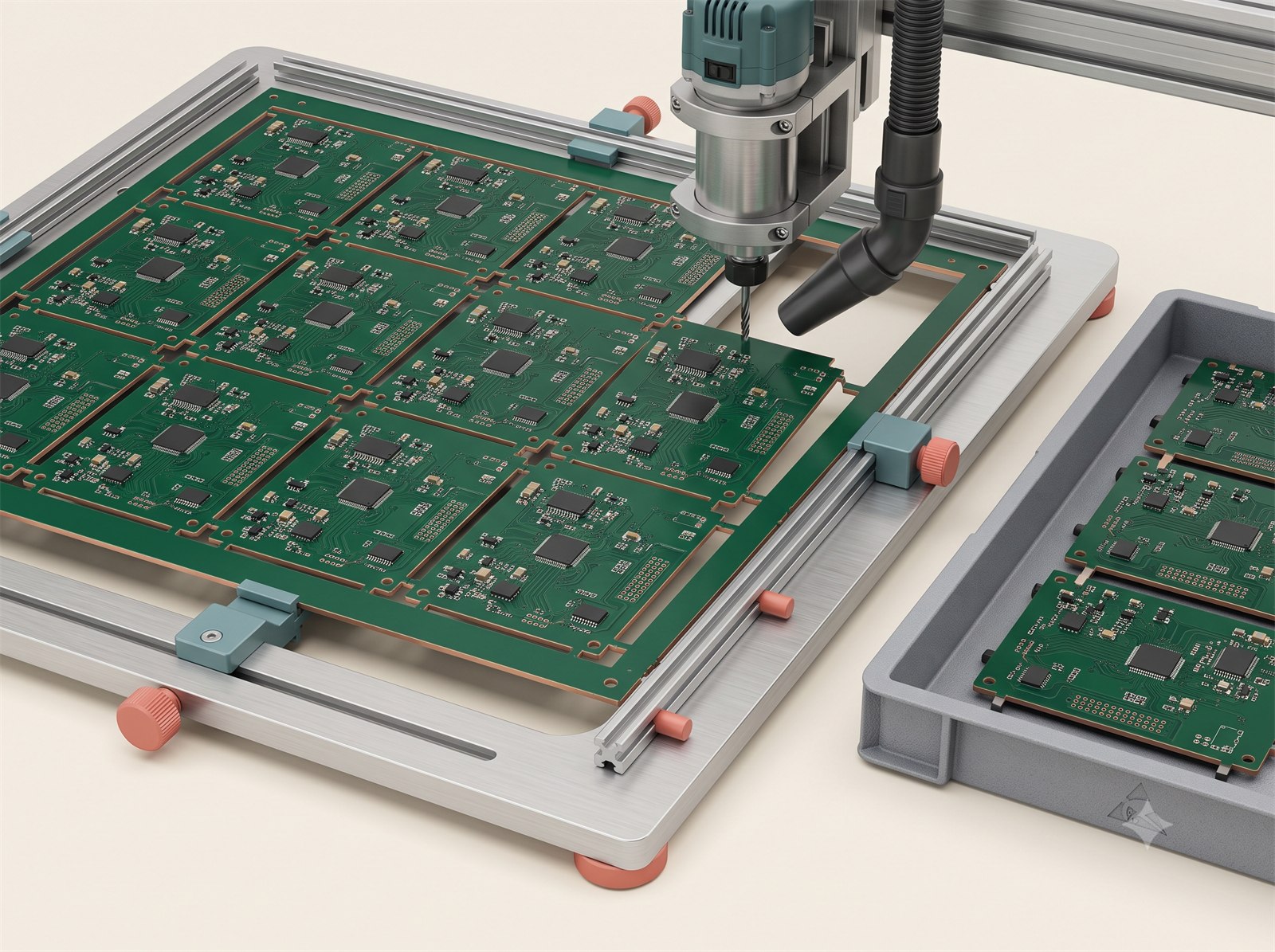 PCB assembly service
Depanel before delivery
Choose whether rails and array breakaways are removed before shipment.
Read the guide ↗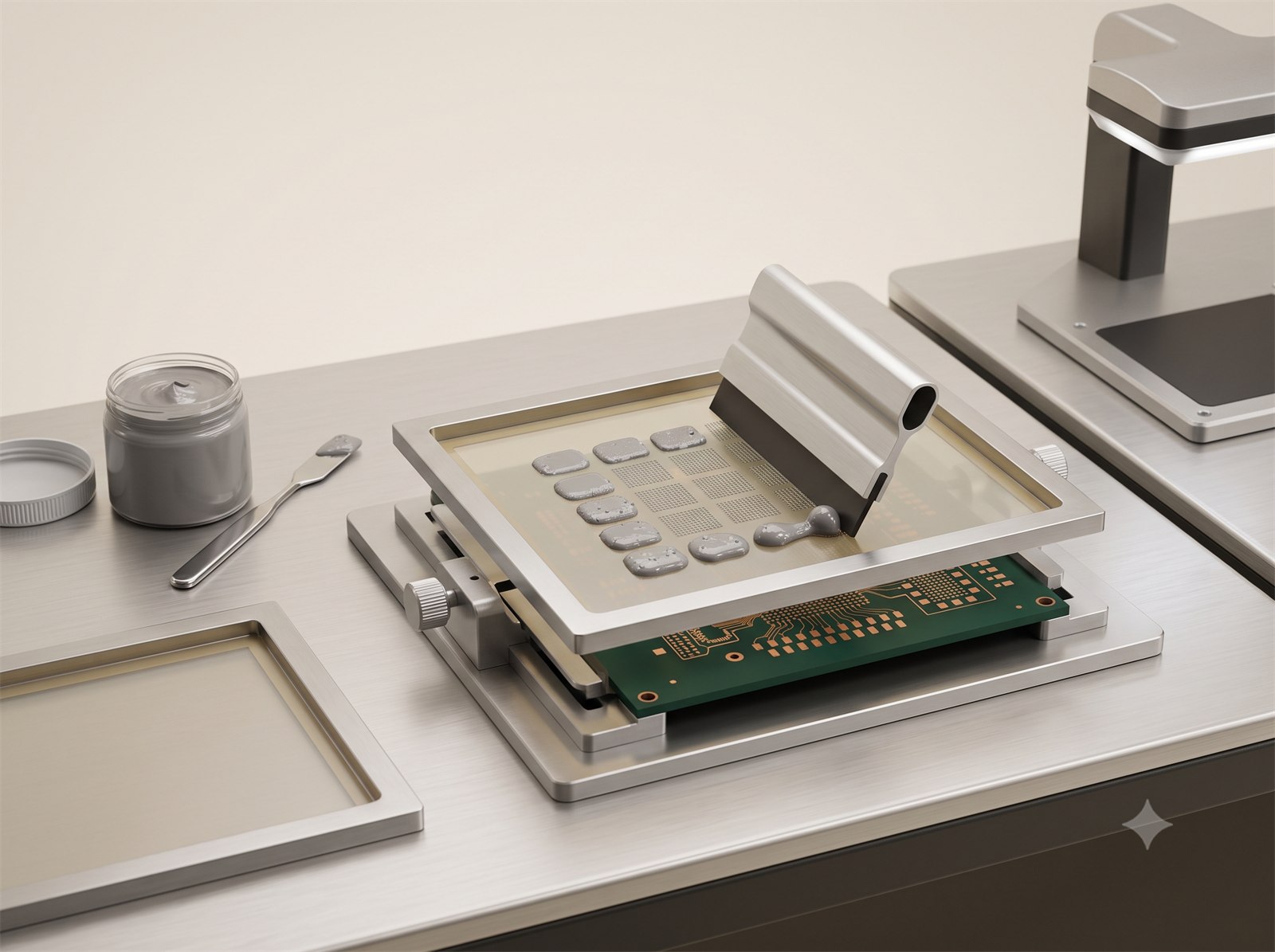 PCB assembly service
Solder paste
Match alloy and reflow temperature to the board and components.
Read the guide ↗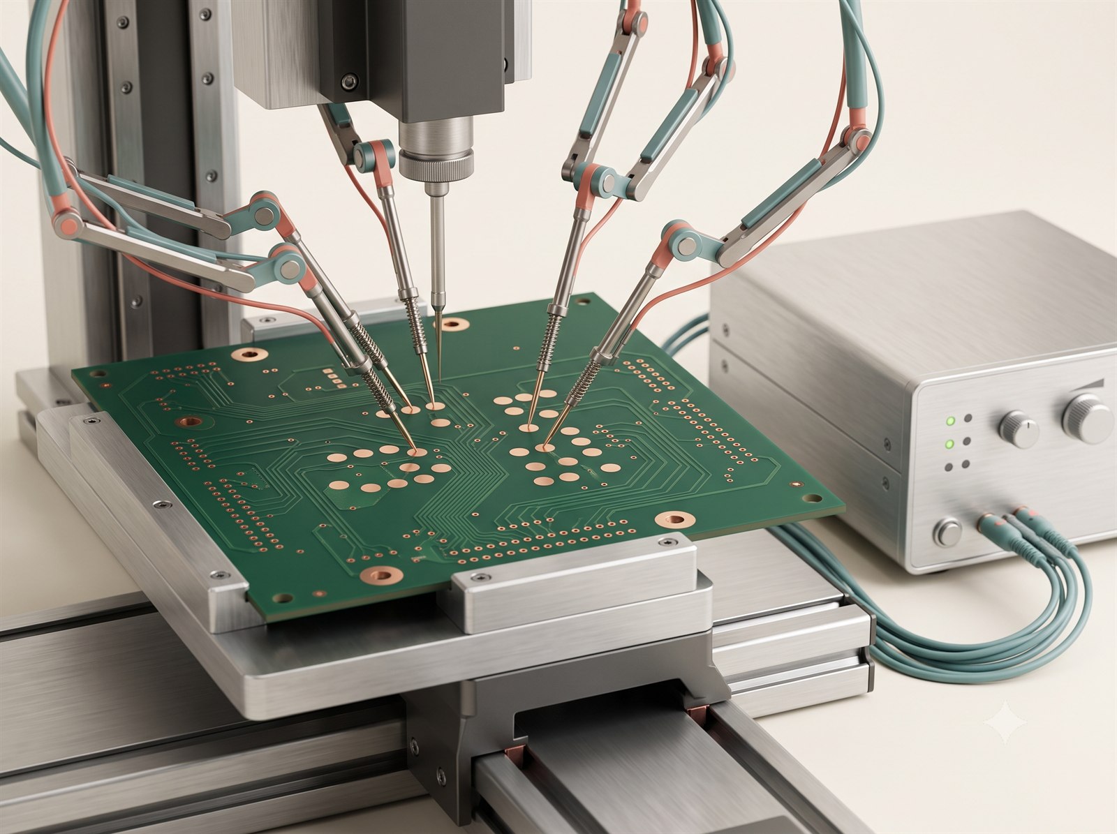 PCB assembly service
Flying probe test
Check accessible circuit nodes without a dedicated fixture.
Read the guide ↗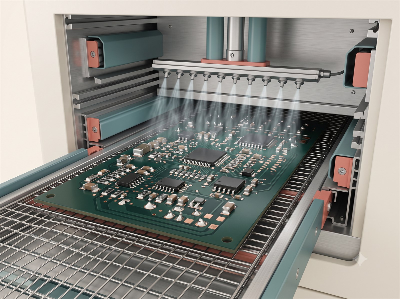 PCB assembly service
Nitrogen reflow soldering
Use controlled atmosphere when process evidence justifies it.
Read the guide ↗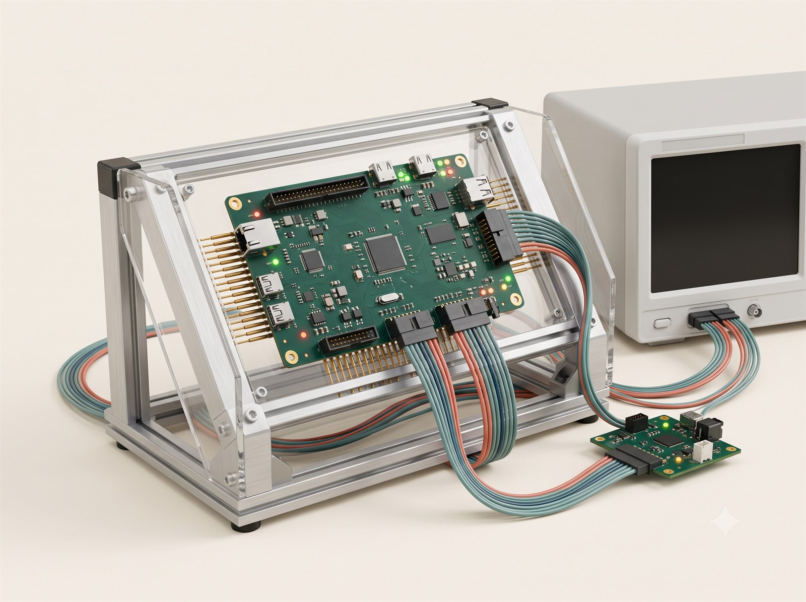 PCB assembly service
Function test
Verify defined powered behavior with a safe controlled procedure.
Read the guide ↗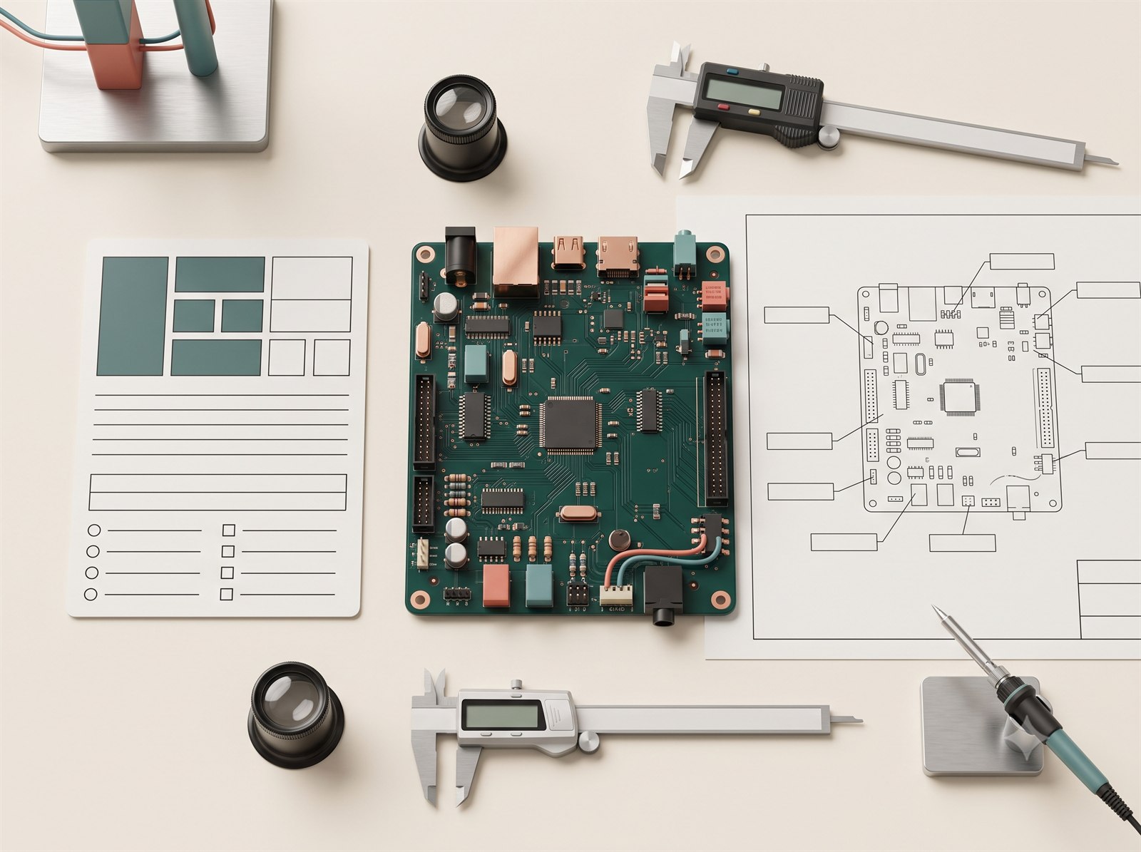 PCB assembly service
Assembly remark
Capture one concise assembly requirement not covered elsewhere.
Read the guide ↗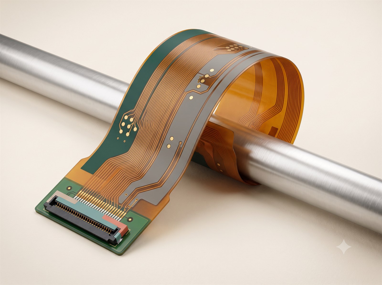 Flex and specialised materials
Substrate type
Choose the dielectric construction that carries the flex-circuit copper.
Read the guide ↗ Flex and specialised materials
Copper type
Match foil ductility and surface profile to bending and signal needs.
Read the guide ↗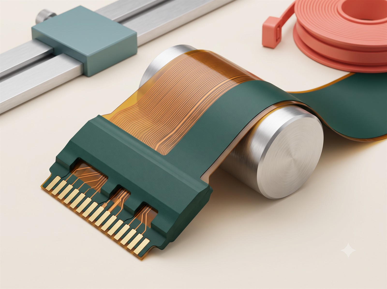 Flex and specialised materials
Coverlay thickness
Coordinate polyimide, adhesive, copper and pad openings.
Read the guide ↗ Stack-up engineering
Stack-up type
Choose the lamination arrangement that supports the design.
Read the guide ↗ Stack-up engineering
Layer stack-up
Define copper, dielectric materials and thicknesses in order.
Read the guide ↗ Design data
EDA software
Prepare neutral fabrication outputs with correct units and origins.
Read the guide ↗ Flex mechanics
Stiffener
Reinforce connector, component or mounting zones deliberately.
Read the guide ↗ Flex signal integrity
EMI shielding film
Add a grounded shielding layer with defined openings and sides.
Read the guide ↗ Flex mechanics
Cutting method
Select outline formation from tolerance and edge-quality needs.
Read the guide ↗ Flex documentation
Silkscreen on stiffener
Place readable markings on a reinforced flex region.
Read the guide ↗ Flex signal integrity
Grounding
Define how shielding and conductive structures reach reference.
Read the guide ↗ Flex mechanics
Polyimide stiffener thickness
Balance local support with the intended connector thickness.
Read the guide ↗ Flex mechanics
FR-4 stiffener thickness
Create rigid local support with a controlled total build.
Read the guide ↗ Flex mechanics
Stainless-steel stiffener thickness
Use thin high-stiffness reinforcement with explicit isolation.
Read the guide ↗ Flex installation
Adhesive tape thickness
Set installation stand-off and bonding compliance.
Read the guide ↗ Flex handling
Polyimide stiffener lift tab
Add a graspable handling feature without disturbing the bend zone.
Read the guide ↗ Flex handling
FR-4 stiffener lift tab
Define a rigid handling extension and its removal method.
Read the guide ↗ Flex handling
Stainless-steel stiffener lift tab
Control a thin rigid tab, its edges and electrical isolation.
Read the guide ↗ Flex installation
Adhesive tape pull tab
Expose a liner edge for predictable clean installation.
Read the guide ↗ Flex connectors
Gold-finger thickness
Match the reinforced contact region to the mating connector.
Read the guide ↗ Metal-core materials
Thermal conductivity
Use the complete through-board thermal path, not one number.
Read the guide ↗ Metal-core materials
Breakdown voltage
Coordinate dielectric withstand with safety spacing and test.
Read the guide ↗ Metal-core materials
Copper structure
Choose the conductive arrangement for current and heat spreading.
Read the guide ↗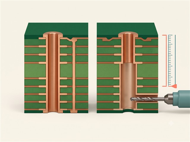 High-speed PCB
Backdrill
Remove unused via stub length from a controlled channel.
Read the guide ↗ Mechanical interconnect
Press-fit hole
Match finished hole and plating to the compliant-pin system.
Read the guide ↗ Stack-up engineering
Specify stack-up
Lock a construction when performance depends on it.
Read the guide ↗ Signal integrity
Impedance test report
Record coupon measurements against controlled-impedance targets.
Read the guide ↗ HDI PCB
HDI structure
Define sequential lamination and microvia build-up complexity.
Read the guide ↗