
The short answer
What this setting controls
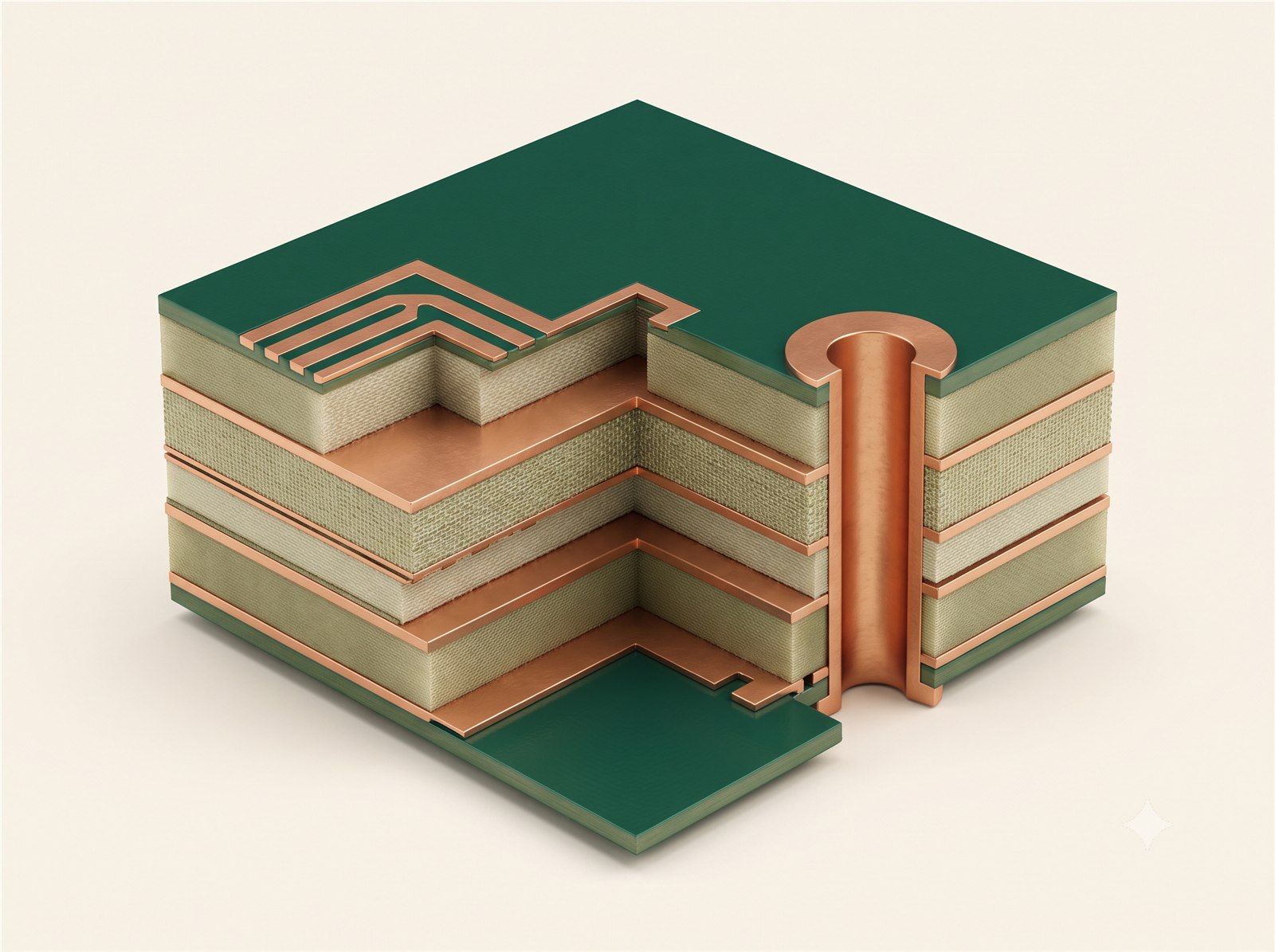
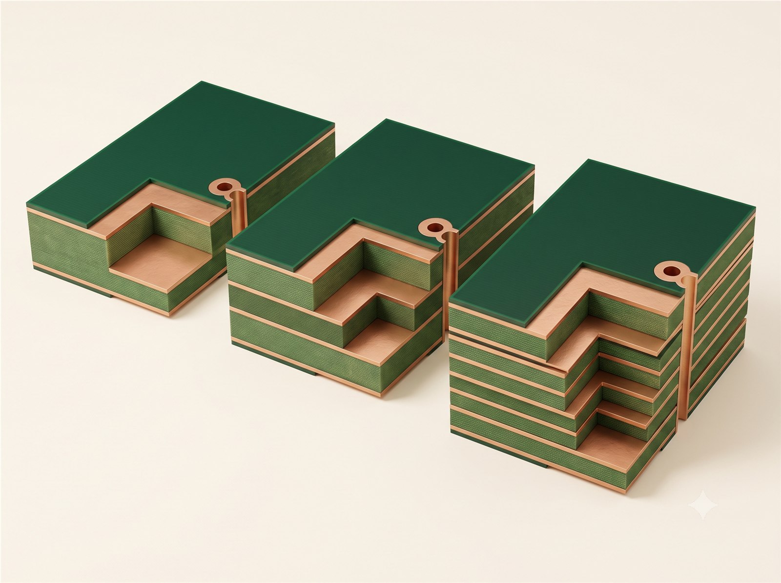
A two-layer board has copper on the top and bottom. A multilayer board adds inner copper planes for routing, power and ground. More layers are not automatically better; they are useful when they create a cleaner, manufacturable layout.
Select a layer count together with the approved stack-up, impedance targets, return-current strategy, copper weights and via technology. The available thicknesses and material families can narrow as the stack becomes denser.
Options in the order form
How the available choices differ
| Choice | Use it for | Engineering note |
|---|---|---|
| 1 layer | Very simple, low-density circuits | No continuous opposite-side return plane; routing and EMC options are limited. |
| 2 layers | Most prototypes and modest-density products | Use the opposite layer deliberately for return paths rather than treating both sides as interchangeable routing space. |
| 4–6 layers | Dense digital, mixed-signal and stronger power integrity | Allows dedicated reference and power planes with a controlled stack-up. |
| 8+ layers | High pin-count, high-speed or tightly constrained designs | Requires explicit stack-up, impedance, via-stub and lamination planning. |
Compatibility
What can change with this selection
- Changing layers can reset incompatible material, thickness, copper and advanced choices.
- A layer count read from Gerber data is evidence about the file, but the chosen build still needs a manufacturing check.
- Layer count and stack-up jointly control impedance, reference planes, dielectric thickness and via construction.
Practical recommendation
How to make the decision
- Keep the lowest layer count that provides a reliable return path and routing density.
- Use a dedicated ground plane when it improves return current, EMC or power integrity.
- For high-speed or dense designs, bring the layer count and stack-up to review before freezing the quote.
Before release
Check these points before adding the quote to cart
- Confirm the selected value matches the released Gerber, drawing, stack-up, BOM or assembly plan.
- Review any fields that changed automatically after this selection.
- Check the board preview and server-calculated estimate before adding the quote to cart.
- Keep the lowest layer count that provides a reliable return path and routing density.
- Use a dedicated ground plane when it improves return current, EMC or power integrity.
- For high-speed or dense designs, bring the layer count and stack-up to review before freezing the quote.
Frequently asked questions
Answers for ordering and design review
Does a two-layer board always cost less?
Often, but not always. Area, quantity, copper weight, finish, testing and special processes can dominate the total.
Why can some layer counts be unavailable?
A material family or process may not support every stack-up. The interface removes combinations that cannot be represented reliably.
Should every power rail have its own plane?
Not automatically. Use planes where they improve return paths, impedance, current distribution or routing; small or low-current rails may be better routed deliberately.
Why is an option disabled?
The current material, geometry, layer count, quantity or another selected process makes that combination unavailable. Change the controlling selection or revise the design package rather than trying to bypass the disabled state.
Can I rely on the online choice as final manufacturing approval?
No. The interface screens known combinations and requests pricing, while final manufacturability remains subject to the released files and technical review.
What should I record outside the order form?
Put controlled requirements in the fabrication drawing, assembly drawing, stack-up, BOM or acceptance plan. Use Special instructions only for a concise pointer to that controlled requirement.
Will changing this update other selections?
It can. The order form re-evaluates compatibility and may replace a now-invalid dependent choice before requesting a fresh server-side estimate. Review every highlighted or automatically changed field.
What if the design requires an option that is not offered?
Do not approximate it with a different label. Recheck the controlling material and geometry, document the actual requirement, and request technical review before placing the order.
Useful engineering tools
Calculators and preparation guides
Further reading
Standards and technical references
Use the latest applicable revision and your organisation’s controlled requirements when a standard forms part of product acceptance.